
 Direct Depth- and Lateral- Imaging of Nanoscale Magnets Generated by Ion Impact
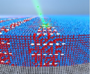
(20 November 2015) Nanomagnets form the building blocks for a variety of spin-transport, spin-wave and data storage devices. In this work we generated nanoscale magnets by exploiting the phenomenon of disorder-induced ferromagnetism; disorder was induced locally on a chemically ordered, initially non-ferromagnetic, Fe60Al40 precursor film using a~2 nm diameter beam of Ne+ ions at 25 keV energy. The beam of energetic ions randomized the atomic arrangement locally, leading to the formation of ferromagnetism in the ion-affected regime. Read more
International Graphene Centre launches in Beijing
(20 November 2015) The China-UK collaborative effort to support the development an international graphene standards and testing centre was officially launched at Zhongguancun Fengtai Science Park, Beijing, China, in October 2015. As the demand for international standards for testing graphene increases, the Centre in Beijing will lay the foundation for the development of graphene industry and high-end applications in China. Read more
 Graphene’s stabilizling influence on supercapacitors
(18 November 2015) Supercapacitors can be charged and discharged tens of thousands of times, but their relatively low energy density compared to conventional batteries limits their application for energy storage. Now, A*STAR researchers have developed an ‘asymmetric’ supercapacitor based on metal nitrides and graphene that could be a viable energy storage solution (“All Metal Nitrides Solid-State Asymmetric Supercapacitors”). Read more
New discovery provides new opportunities for chips
(18 November 2015) A new manufacturing method to create three-dimensional nanostructures has been uncovered by scientists. This revolutionary method enables large-scale production of photonic crystals that can capture light. The discovery also makes it possible to produce chips with additional functions for mobile devices, computers and other applications. Read more
 Stacking instead of mixing improves the energy efficiency of topological insulators
A flexoelectric microelectromechanical system on silicon
(17 November 2015) Flexoelectricity allows a dielectric material to polarize in response to a mechanical bending moment1 and, conversely, to bend in response to an electric field2. Compared with piezoelectricity, flexoelectricity is a weak effect of little practical significance in bulk materials. However, the roles can be reversed at the nanoscale3. Here, we demonstrate that flexoelectricity is a viable route to lead-free microelectromechanical and nanoelectromechanical systems. Read more
Unimolecular Submersible Nanomachines. Synthesis, Actuation, and Monitoring
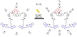 (5 November 2015) Unimolecular submersible nanomachines (USNs) bearing light-driven motors and fluorophores are synthesized. NMR experiments demonstrate that the rotation of the motor is not quenched by the fluorophore and that the motor behaves in the same manner as the corresponding motor without attached fluorophores. No photo or thermal decomposition is observed. Through careful design of control molecules with no motor and with a slow motor, we found using single molecule fluorescence correlation spectroscopy that only the molecules with fast rotating speed (MHz range) show an enhancement in diffusion by 26% when the motor is fully activated by UV light. Read more
Deep-subwavelength Nanometric Image Reconstruction using Fourier Domain Optical Normalization
(5 November 2015) Quantitative optical measurements of deep sub-wavelength, three-dimensional, nanometric structures with sensitivity to sub-nanometer details address an ubiquitous measurement challenge. A Fourier domain normalization approach is used in the Fourier optical imaging code to simulate the full three-dimensional scattered light field of nominally 15 nm sized structures, accurately replicating the light field as a function of the focus position. Using the full three-dimensional light field, nanometer scale details such as a 2 nm thin conformal oxide and nanometer topography are rigorously fitted for features less than 1/30th of the wavelength in size. Read more
Continuous Carbon Nanotube–Ultrathin Graphite Hybrid Foams for Increased Thermal Conductivity and Suppressed Subcooling in Composite Phase Change Materials
(3 November 2015) Continuous ultrathin graphite foams (UGFs) have been actively researched recently to obtain composite materials with increased thermal conductivities. However, the large pore size of these graphitic foams has resulted in large thermal resistance values for heat conduction from inside the pore to the high thermal conductivity graphitic struts. Here, we demonstrate that the effective thermal conductivity of these UGF composites can be increased further by growing long CNT networks directly from the graphite struts of UGFs into the pore space. Read more
Nanotech tools open market for more miniature electronics
(27 October 2015) In order to develop ultra-miniaturised electronic components, ultra-miniaturised capacitors are required. The two-year EU-funded PICS project has developed tools that could soon lead to the mass production of high-density 3D integrated silicon capacitors, creating new opportunities for SMEs to tap demand for miniaturised high performance electronics across a range of sectors. Read more
Lithography and Photomask Technologies Stand at a Crossroads
(27 October 2015) The current optical lithography is expected to give way, at least with the most advanced layers of semiconductor devices, to extreme-ultraviolet (EUV) lithography, multiple-beam electron-beam lithography and direct-write e-beam lithography. Directed self-assembly and nanoimprint lithography are also anticipated to find useful applications in patterning chips.
The standard binary photomask is expected to stay the same size, at six inches by six inches by 0.25 inch, for the next-generation of lithography. Other than that, the proliferation of masks needed for 193i immersion lithography is expected to be alleviated by the introduction of EUV lithography into high-volume manufacturing (HVM), requiring fewer masks and exposures. Read more
Electronics Get a Boost with This Newly Discovered Technique
(21 October 2015) The tiny transistor is a major part of the electronics revolution. Now, Penn State materials scientists have discovered a way to give this bit of tech a big boost by using a new technique to incorporate vanadium oxide, a functional oxide, into the electronic devices. “It’s tough to replace current transistor technology because semiconductors do such a fantastic job,” says Roman Engel-Herbert, assistant professor of materials science and engineering. “But there are some materials, like vanadium oxide, that you can add to existing devices to make them perform even better.” Read more
ASIC Design Made Cost Effective with Low Cost Tools and Masks
(13 April 2015) For smaller projects or companies with modest design budgets, ASIC design is becoming a viable option due to low cost design tools and easy access to flexible, mature IC processes. This is especially compelling for developing mixed-signal ASICs for cost-sensitive sensor applications for the Internet of things (IoT). This paper discusses how costs and risks can be reduced using multi-project wafer services, coupled with affordable design tools for developing mixed-signal ASICs. Read more
High-Performance Analog and RF Circuit Simulation
(13 March 2015) The research group led by Professor Peter Kinget at the Columbia University Integrated Systems Laboratory (CISL) focuses on cutting edge analog and RF circuit design using digital nanoscale CMOS processes. Key challenges in the design of these circuits include block-level characterization and full-circuit verification. This paper highlights these verification challenges by discussing the results of a 2.2 GHz PLL LC-VCO, a 12-bit pipeline ADC, and an ultra-wideband transceiver. Read more